The speaker for this week's seminar is:
11:55am - 12:45pm: Dr. G. Bahar Basim (Invited speaker - UF): A Review on Controlling Nano-Scale Chemically Modified Thin Films for Microelectronics Processes Development
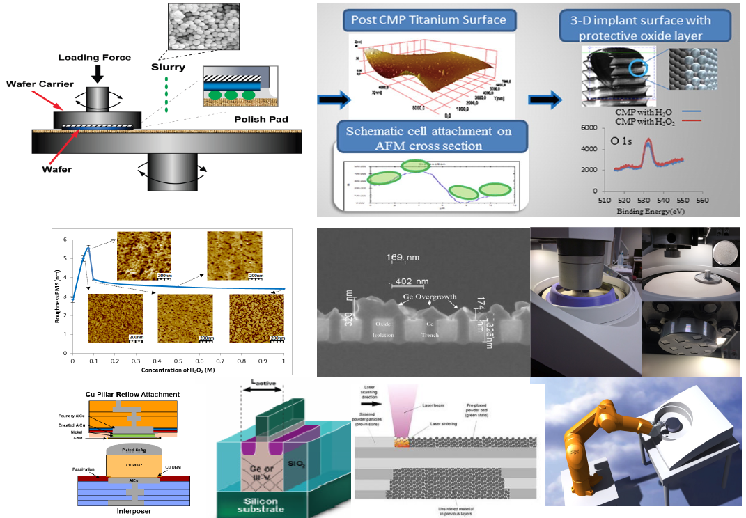
As the microelectronics manufacturing faces the challenges related to Beyond Moore’s scale adaptation, process development has become more challenging. Particularly, for the Chemical Mechanical Planarization (CMP) process, the need for planarizing larger scale wafers at an atomic scale precision with superior removal rate selectivity and zero-defect focus demands a nano-scale control on the process performance. This talk reviews the atomic-scale chemical and mechanical interactions as it applies to traditional as well as the next generation materials in microelectronics manufacturing.
In an attempt to come up with the design criteria for the slurry chemistry, chemically modified layer formation is evaluated on conducting, semiconducting, and insulating materialsas a function of evaluating the nano-scale surface topography and change in surface energy. Metallic films are studied in terms of their corrosion and passivation behavior through macro-scale electrochemical evaluations as well as surface-sensitive characterization techniques such as XRR, XRD, and FTIR. A modeling approach is introduced through Cahn Hilliard Equation (CHE) approximation to the surface energy minimization on the metal-oxide formation by nucleation. Furthermore, the removal rate selectivity properties of the semiconductor materials are discussed on conventional and III-V semiconductors and insulators as a function of chemically modified film alteration. Some high-end applications such as (i) tungsten T-gate transistors, (ii) new liner/barriermaterials, (iii) germanium based high-speed, shallow trench isolation transistors and (iv) high-power transistors and LED applications where III/V semiconductors are deliberated. As a new challenge, 3-D implementations of the CMP process, where the chemically modified nano-films impact the performance of the material, are also introduced. The ongoing research focuses on the packaging level of thin film growth and interface control, implantable microelectronics, and controlling biological interfaces.